|
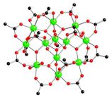
Mn-12 |
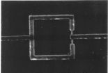
A microSQUID (about 2 micrometer on a side), made of aluminum. |
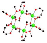
Mn-6 |
|
 |
Earlier Research |
NanoSQUIDs - Development and Applications
The first objective of this project is to miniaturize Superconducting
Quantum Interference Devices (SQUIDs) to the nanometer regime ("NanoSQUIDs").
SQUIDs are employed as ultra-sensitive magnetic flux detectors in research
and industrial applications. Reducing the size of SQUIDs to the micrometer
regime ("MicroSQUIDs") has yielded important scientific results in the
characterization of magnetic nanoparticles.1,2 A further reduction
in size to the nanometer regime ("NanoSQUIDs") brings this powerful technique
to the scale of magnetic single domain particles and individual macromolecules
where novel quantum mechanical properties are relevant. NanoSQUIDs are
expected to be useful for applications in magnetic characterization, in
particular where small spatial resolution or arrays of localized detectors
are required.
The second objective is to use NanoSQUIDs for the characterization
of molecular nanomagnets. While some initial work in this direction has
already yielded interesting results,2 a number of important
experiments are yet to be implemented. These experiments are driven by
new and different molecular nanomagnets as well as the desire to reduce
the number of molecular nanomagnets in the system being investigated.
More long-term, the third objective is to implement useful spintronics
devices, where NanoSQUIDs and molecular nanomagnets are integrated. The
production of NanoSQUIDs is part of a decade-long process of miniaturization
of electronic devices, typically referred to as the top-down approach.
More recently, largely spurred by important advances in molecular chemistry,
the production of appropriate molecular compounds has opened a second alternative
towards the goal of creating small, but controlled, systems: the molecular
self-assembly into nanoscopic structures, typically referred to as the
bottom-up approach. Any useful device created by the bottom-up approach,
however, has to be connected to the macroscopic world. Such a connection
requires an interface technology between the top-down and the bottom-up
approach. In the case of a magnetic system, a NanoSQUID can provide this
interface, as it allows for individual access to information in a molecular
nanomagnet. Such an integrated system also has the potential of a model
quantum computation system3 with integrated readout technique.
This project is expected to develop significant synergy with a recently
awarded NSF Nanoscience Interdisciplinary Research Team4 at
the physics and chemistry departments of Texas A&M University, which
is working on the chemical synthesis and physical properties of molecular
nanomagnets.
1 W. Wernsdorfer et al., Phys. Rev. B 55, 11552 (1997). W.
Wernsdorfer et al., Phys. Rev. Lett. 78, 1791 (1997). And further work
by same group of authors.
2 W. Wernsdorfer and R. Sessoli, Science 284, 133 (1999).
W. Wernsdorfer et al., Phys. Rev. Lett. 82, 3903 (1999). And further work
by same group of authors.
3 J. Tejada et al., cond-mat/0009432, M. Leuenberger et
al., cond-mat/0011415.
4 Molecular Nanomagnets: Magnetic and Electronic Properties
of Novel Magnetic Nanostructures and Nanostructured Materials, D.G. Naugle
(PI), G. Agnolet, F.A. Cotton, K.R. Dunbar and V.L. Pokrovsky (duration
2001-2005).
|
|
|
The Spin Hall Effect
The objective of this project is to detect the recently postulated1
Spin Hall Effect (SHE), a physical effect of fundamental importance, which
allows the study of pure spin currents and the characterization of spin
properties in materials.2 It is a topic of considerable pure
and applied interest.
To understand the Spin Hall Effect we revert to the Anomalous Hall
Effect (AHE).3 In ferromagnetic metals, the Hall resistivity
empirically follows ρH=RoB+4 RsM with
B being the applied magnetic field, M the magnetization per unit volume
and Ro and Rs the ordinary and anomalous Hall coefficient respectively.
The first term describes the ordinary Hall effect present in all conductors
and resulting from the Lorentz force (Figure 1a). The second term describes
the anomalous RsM with
B being the applied magnetic field, M the magnetization per unit volume
and Ro and Rs the ordinary and anomalous Hall coefficient respectively.
The first term describes the ordinary Hall effect present in all conductors
and resulting from the Lorentz force (Figure 1a). The second term describes
the anomalous
|
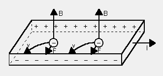
Figure 1: a) Ordinary Hall Effect. |
|
contribution in ferromagnetic materials, which typically
exceeds the ordinary Hall effect contribution. The microscopic origin of
the AHE is controversial. Explanations like the side jump mechanism and
skew scattering by impurities or phonons have been considered.3
Beyond the controversy in origin, the existence of the AHE is experimentally
beyond doubt, which provides a sufficient basis for the current discussion.
The existence of the AHE indicates that electrons, carrying a spin (and
a magnetic moment m), are subject to a transverse force F if they move
in a longitudinal current (Figure 1b). Furthermore, electrons with opposing
spin directions are subjected to a force in opposing directions. In a ferromagnetic
material an applied magnetic field B produces a net magnetization, i.e.
more carriers with spin aligned to the applied field than counter aligned.
This imbalance of itinerant carrier spins leads to a spin and charge imbalance
in the perpendicular direction, which gives rise to the anomalous Hall
voltage (Figure 1b).
|
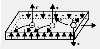
Figure 1: b) AHE contribution in a material with net magnetization. More carriers are deflected to one side, leading to a spin and charge imbalance. |
Typically, only the charge imbalance is detected.
The spin imbalance is, however, a necessary condition for any spin dependent
microscopic description of the AHE.
Next we will focus on the situation which gives rise to the SHE, a
material without magnetization and without applied magnetic field. In a
material without magnetization, the number of carriers with spin up balances
the number of carriers with spin down (Figure 2). Consequently, the same
number of carriers is
|
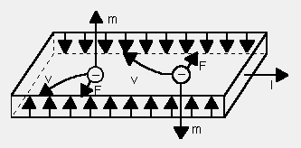
Figure 2: Spin Hall Effect. In a material without magnetization, the number of carriers with spin up equals the number of carriers with spin down. The same mechanism that leads to the AHE scatters spin up carriers preferentially to one side, while spin down carriers are scattered preferentially to the other side. The resulting spin imbalance leads to a spin potential VSH between opposing sides of the strip. |
scattered to one side of a current carrying strip
than to the other and no charge imbalance between the different sides of
the strip exists. There is, however, an imbalance of spins between the
different sides of the strip, since spin up carriers are preferentially
scattered to one side, while spin down carriers are preferentially scattered
to the other. The resulting spin imbalance gives rise to a spin potential
VSH, while the electronic potential is constant as one moves from one side
of the strip to the opposite side (Figure 2). VSH is a direct consequence
of same microscopic models, leading to the AHE.
To detect the SHE, Hirsch suggested an elegant analogy to a double
Hall effect device. The idea is that a perpendicular cross strip connects
the opposite sides of the current carrying strip. In case of double Hall
effect at B>0 (Figure 3a), the electronic
|
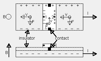
Figure 3: a) Same device in B=0. The SHE leads to an electronic potential between point 1 and 2, though no Lorentz forces are acting on carriers. |
|
potential in the current carrying
strip induces a perpendicular current in the cross strip, which itself
is subject to the Lorentz force. Consequently, an electronic potential
between point 1 and point 2 in Fig. 3 a exists. In case of the SHE (at
B=0), the spin imbalance produced in the current carrying strip migrates
into the opposite ends of the cross strip (Figure 3b). Inside the
|
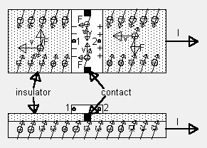
Figure 3: b) Double Hall Effect in a tri-layer structure. The top cross strip is insulated from the current carrying strip underneath except for two contact points. Lorentz forces lead to a potential between point 1 and 2. |
cross
strip there is, however, no reason why a spin imbalance should remain.
Consequently, a spin current flows in the cross strip which itself is subject
to the spin scattering mechanism. As can be seen in the cross strip of
Figure 3b, electrons of opposing spin direction are flowing towards each
other to eliminate the spin imbalance. Due to the same force that lead
to the spin separation in the current carrying strip, they are scattered
towards the same side of the cross strip. The result is an electronic potential
between point 1 and point 2, which can be measured as a voltage. Hirsch
calculates the size of the expected voltage in Aluminum to be 58nV, based
on lithographic length scales, idealized interfaces, perfect alignment
and work by Johnson and Silsbee.4
Discovering the postulated SHE and investigating its details will have
several benefits for fundamental and applied physics. Fundamentally, this
experiment would produce a pure spin current and would investigate the
interrelations of spin and charge currents. Furthermore it would show that
a skew scattering mechanism exists even in a paramagnetic material and
is thus a more general phenomenon. This would aid in the understanding
of the AHE, one of the more significant outstanding issues in condensed
matter physics. On the applied side, this project would provide information
on the spin diffusion length and its dependence on material properties.
The understanding of the material dependence of spin diffusion length and
spin-related scattering will aid technologists in the selection of materials
for spin electronics devices.
1 J. E. Hirsch, Phys. Rev. Lett. 83, 1834 (1999).
2 S. Zhang, Phys. Rev. Lett. 85, 393 (2000).
3 C. M. Hurd, The Hall Effect in Metals and Alloys",
Plenum, New York, 1973, Chapter 5.
4 M. Johnson and R. H. Silsbee,
Phys. Rev. Lett. 55, 1790 (1985);
Phys. Rev. B 37, 5312 (1988).
|
|
|
A Metal-Insulator transition in 2-dimensional GdxSi1-x?
This project has the following objectives:
1. To help answer the fundamental
question: Is there a metallic state and thus a Metal-Insulator transition
in 2 dimensions? And if so,
2. To measure the density of states in an in-situ
tunable material in 2 dimensions and determine the critical exponent.
The existence of a Metal-Insulator transition in 2 dimensions is a disputed
topic. While the existence of a metallic state in 3 dimensions is beyond
doubt there is strong evidence that the existence of any amount of disorder
will lead to an insulating state in 1 dimension. The 2-dimensional case
is of particular interest since it is believed to be a borderline case.
While it has been thought for some time, that a metallic state cannot exist
in 2 dimensions, subsequent work has put this conclusion in doubt.2
Furthermore, there have been several experimental results that suggest
the existence of a metallic state in 2 dimensions.2 Here I propose
an experiment, which measures the density of states of a 2-dimensional
material, whose disorder can be reversibly tuned in-situ. Working as a
post-doc with Bob Dynes at the University of California, San Diego and
in collaboration with Frances Hellman (UCSD), we have recently conducted
the equivalent experiment in 3 dimensions.3 We found, that the
results in the limiting metallic and insulating cases are well described
by existing theories and that the density of states in the transition region
could be determined to unprecedented quantitative precision (see Figure).
|
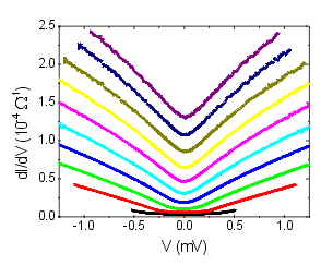
Figure: The density of states of GdxSi1-x at the
Metal-Insulator Transition. |
|
As a result, the critical exponent of the density of states in the critical
regime of the 3-dimensional metal insulator transition could for the first
time be determined (it is 2).4 This project is an ongoing collaboration
with Bob Dynes, Frances Hellman and co-workers.
1 P. A. Lee and T. V. Ramakrishnan,
Rev. Mod. Phys. 57, 287
(1985).
2 E. Abrahams, S. V. Kravchenko and M. P. Sarachik,
Rev.
Mod. Phys. 73, 251 (2001).
3 W. Teizer, F. Hellman and R. C. Dynes,
Phys. Rev. Lett.
85, 848 (2000).
4 W. Teizer, F. Hellman and R. C. Dynes,
to be published.
|
|
|
|
© Copyright 2018 Winfried Teizer
|
|
|
|